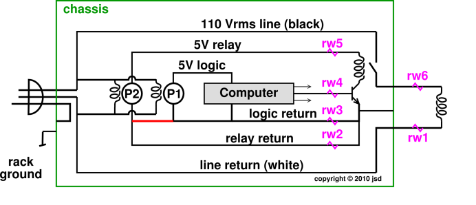
Figure 1: Single Point Grounding; Negligible Resistive Coupling
The ways that noise can couple into a circuit can be classified as
Figure 1 shows a circuit that follows basic sound design principles. There is minimal resistive coupling.
Some salient features of this circuit include:
This is not claimed to be an advanced ultra-low-noise design. This is just the basic price of admission.
Non-experts sometimes think that the low side of the power supply is the natural place where things should be grounded, but in figure 1 the one place where all the current loops are tied together is way over on the right, at the emitter of the driver transistor.
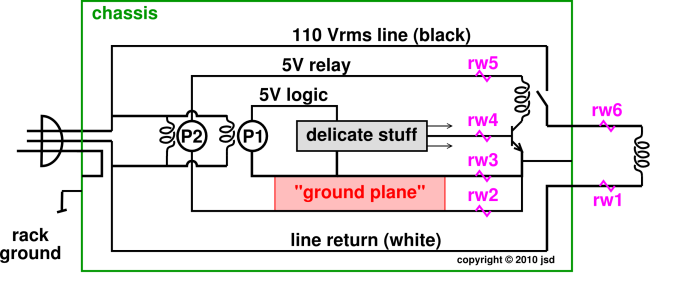
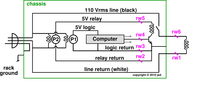
In contrast, figure 2 shows a circuit that suffers from a nasty resistive coupling.
The problem here is that the heavy current that flows through the relay coils causes an IR drop in (rw2 ∥ rw3). This causes some of the logic levels to be referenced to an unreliable ground level, leading to intermittent logic errors.
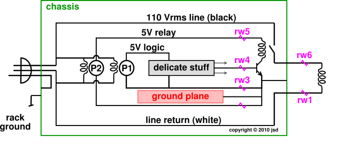
A similar problem can be seen in figure 3.
Non-experts sometimes think that if the have something called a “ground plane” they can use it as some sort of cloaca major such that they can flush whatever current they like into it without worrying. Having a ground plane is fine if you use it properly. A ground plane works best if it is an equipotential. It is an equipotential if and only if there is negligible current flowing through it. Connecting the ground plane to logic return at one point is sufficient to guarantee no large currents in it. The power return buses need to be managed carefully and separately, as in figure 4.
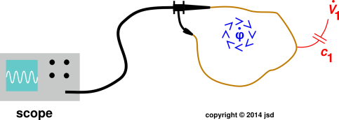
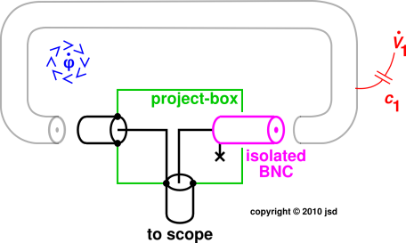
A quick way to make a rough estimate of the time-dependent magnetic field is shown in figure 5. All you need is an oscilloscope and a loop of wire.
This setup is not ideal, because if there are large time-dependent electric fields, they can couple to the circuit via parasitic capacitances (such as c1). Depending on the resistance of the measuring circuit, this can lead to parasitic IR voltages that mess up the measurement of φ•.
If you want a more accurate measurement of φ•, you can improve the circuit, as shown in figure 6. In particular, build a small box to which you can attach a piece of standard coax.
Start with a small metal “project box” as diagrammed in green. Add three BNC connectors. Two of them are regular non-isolated “self-grounding” BNC connectors (shown in black) such that the shield is connected to the metal box at these points. The third connector is an isolated BNC (shown in magenta) that leaves the shield completely open-circuited at this point, as indicated by the × in the figure. Wire things up as shown.
You can keep the little box in your bag of tricks. When it comes time to use it, connect a piece of coax to it, as shown in gray in the diagram. The φ• will induce a voltage in the inner conductor of the coax, which you can observe using a scope.
The φ• will also induce a voltage in the outer conductor of the gray coax, but you don’t care, because it does not appreciably couple to the thing you are measuring.
Note that grounding the outer conductor at point × would be a disaster. It would create a shorted turn, i.e. a one-turn shorted secondary winding. The φ• would induce a humongous current in this loop, possibly on the order of amps. In accordance with Lenz’s law this could significantly interfere with what you’re trying to measure.
The reason why you might want a coax (as opposed to the unshielded wire shown in figure ??) is so that capacitively coupled interference, as represented by c1, will be captured by the outer conductor, i.e. the shield. This injects a few microamps of noise into the shield, but we don’t care, because gets drained via a low-impedance path to ground, and does not appreciably couple to the thing we are measuring.
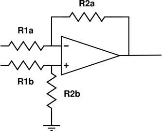
Figure 7 is an ordinary diagram of an ordinary analog subtractor circuit. This is the sort of diagram you might find in an introductory textbook. This circuit may or may not be something you are interested in per se. However, as we shall see, it is representative of a wider class of circuits, and allows us to explore a number of fundamental grounding and shielding concepts.
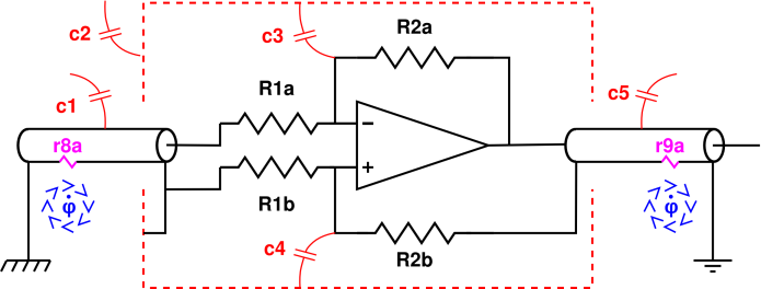
Figure 7 is a fancier diagram version of figure 7. In some over-idealized sense it pertains to the “same” circuit, but depicts quite a number of additional details, including: