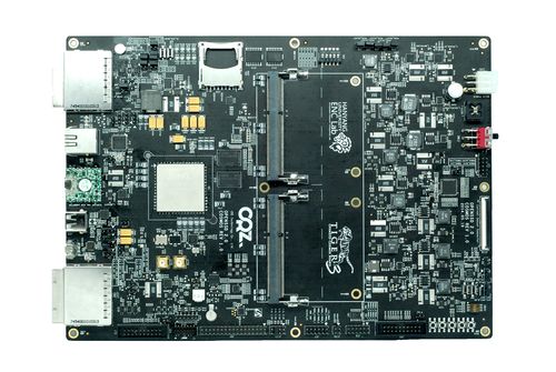
Figure 1: Single-Board Computer with Bare Flash
Copyright © 2015 jsd
Suppose you want to store some private data on an electronic device such a phone, tablet, computer, or the like. Sometimes it suffices to encrypt the data, but just leaves us with the question of how to protect the privacy of the keys. At some point it becomes necessary to erase something, and to be absolutely sure it is erased. Erasing a smallish thing like a key is easier than erasing a large thing such as a one-time pad.
Real security depends on mathematics, physics, electrical engineering, computer programming, human factors, et cetera. It requires tremendous attention to detail, as discussed in the excellent reference 1.
Concepts such as security and reliability mean different things to different people. Heretofore, in the computing and data-storage business, there has been great emphasis on protecting against loss of information ... and much less emphasis on protecting against loss of privacy. Note that these two things in some ways opposites, insofar as protecting privacy requires destroying some information.
On the other hand, nowadays you cannot protect your information unless you also protect your privacy. That’s because if somebody steals your passwords and cryptographic keys, they can destroy your information and everything else.
Let’s consider the practical details involved in using an electronic device (such as flash memory) to implement a one-time pad. We assume you have a good method for randomly generating numbers to be stored on the pad. (Random generation is highly nontrivial, but the details are outside the scope of this document.) Then it is quite straightforward to write a program that performs encryption and decryption by XORing a message with the pad file.
If you were to use the XOR program “as-is”, it would flunk the silk-or-cyanide test as discussed in reference 1. Specifically, we should consider the following scenario:
In this scenario, you lose spectacularly. You have gained nothing by encryption, and all you really did is call attention to yourself. The XOR program implements the encryption and decryption, but fails to implement the one-time property. The pad is not a one-time pad. There is no forward secrecy.
This stands in contrast to a scenario where every bit of the pad was zeroized as soon as it was used. When the bad guys catch you, they simply cannot force you to reveal the keys. They will still torture you, and demand that you reveal the contents of the encrypted messages, but you are free to lie to them, because they cannot tell whether or not your encrypted messages agree with what you are saying.
It not very easy to fix problem #1. In some vague theoretical sense, the solution is to obliterate the stored key, immediately after it is used. However, when we come to the non-vague practical details, this is not so easy to do.
There are many reasons why this is hard, and will always be hard. As the saying goes: Encryption is easy, but security is hard. We must emphasize the following distinction:
| It is easy to write an XOR program that just encodes and decodes. | It is vastly harder to implement a true OTP system that not only encodes and decodes but ensures that the pad will be used only once. |
In particular, on a mass-storage device, the naïve logical approach is to do something like “seek(N) ; read() ; seek(N) ; write()” ... which is supposed to zeroize the block immediately after it is used. On some simple devices this works fine, but on other devices it is guaranteed to not work.
In particular, let’s focus attention on flash-based mass storage. Some of the issues are discussed in reference 2, and references therein. The first thing to realize is that the standard logical-block-addressing (LBA) interface presented by SD cards, USB sticks, eMMC modules, SSD drives, etc. is highly abstract, and does not closely match the physics of the underlying transistors. There is a so-called flash translation layer (FTL). In particular, if you write the same LBA block 1000 times, it is virtually guaranteed that the data will go to 1000 different places on the chip. This is a consequence of the wear-leveling strategy implemented by the controller that is built into the card/stick/module/drive/whatever. In addition to wear-leveling there is ECC and bad-block replacement. The controller does not ordinarily give you direct access to the bits on the chip, but an attacker with modestly specialized hardware (as in reference 2) can bypass the controller and see the raw data ... including the data that you tried to overwrite.
Tangential remark: Modern magnetic disks controllers have their own wear-leveling and bad-block replacement issues, but I’d rather concentrate on flash memory for the moment.
At the moment (late 2015), there are solutions to this problem.
| I’m not sure how long the solutions will remain viable. | Any solution is better than none. |
| As discussed in reference 3, current-generation flash chips are so complex and so variable that for almost all practical purposes you need a mated pair: memory chip plus controller. I reckon this will only get worse, for the foreseeable future. | At the moment, the window has not quite closed on previous-generation flash chips. These chips have a reasonably simple, standardized behavior. |
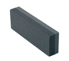
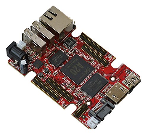
Figure 1 shows an Olimex single-board computer. The processor talks directly to a NAND flash chip, which makes it relatively easy to implement enhanced privacy. The board also has a considerable variety of I/O interfaces.
I have no experience with the board in figure 1, and am not endorsing it, but only offering it as an existence proof. At first glance it appears to be comparable to a Raspberry Pi or a BeagleBone, but more privacy-friendly, because it provides direct access to the flash chip, whereas the others interpose an opaque flash-controller chip.
You can talk to flash chips using open-source drivers. The Linux “MTD” drivers are an example. In particular, /dev/mtdblock0 provides access to the bare flash chip. It would be a SMoP (Small Matter of Programming) to use this to store, read, and obliterate crypto keys (including the one-time pad keystream).
If you cannot immediately lay hands on bare flash hardware, you can simulate it using the linux “nandsim” driver. Reference 4 is an example of some nice crypto-related work that used the nandsim driver. That paper has a good discussion of the underlying technical issues, and also a useful list of references.
Some older phones used bare flash chips. However, newer and/or fancier phones use eMMC modules, so the /dev/mtdblock0 approach no longer works.
Some wireless routers use bare NAND flash chips, and some of these can run DD-WRT, so that might be another platform that permits cryptologically secure erase. If you already needed such a router for other reasons, you incur zero incremental hardware cost.
There is “some” support for open-source NAND flash controllers,
for example:
http://www.openssd-project.org/wiki/The_OpenSSD_Project
http://www.openssd-project.org/wiki/Cosmos_OpenSSD_Platform
http://www.openssd-project.org/wiki/Jasmine_OpenSSD_Platform
One could use that to develop an privacy-enhanced mass-storage device with an ePCI and/or SATA interface. Here are three possible approaches, in order of increasing fanciness:
The third approach is trickier, but is by no means impossible, as discussed in section 2.
Another approach, as discussed in reference 3, is to hack the controller chip within an SD card. This is not easy at the moment, because there’s no systematic method for obtaining a hackable SD card.
On the other hand, looking forward, one could imagine a scenario where the manufacturer actually supports open-source firmware on a flash controller (in analogy to the way that some router manufacturers support DD-WRT). This could apply to SD cards, USB sticks, eMMC modules, SSD drives, et cetera. The hardware discussed in section 1.4.2 might make it easier to prototype the firmware.
There already exists an Open Nand Flash Interface; see http://www.onfi.org/.
There is also OpenNFM i.e. Open Nand Flash Manager firmware https://code.google.com/p/opennfm/
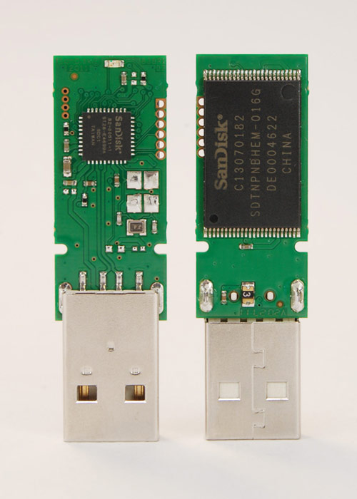
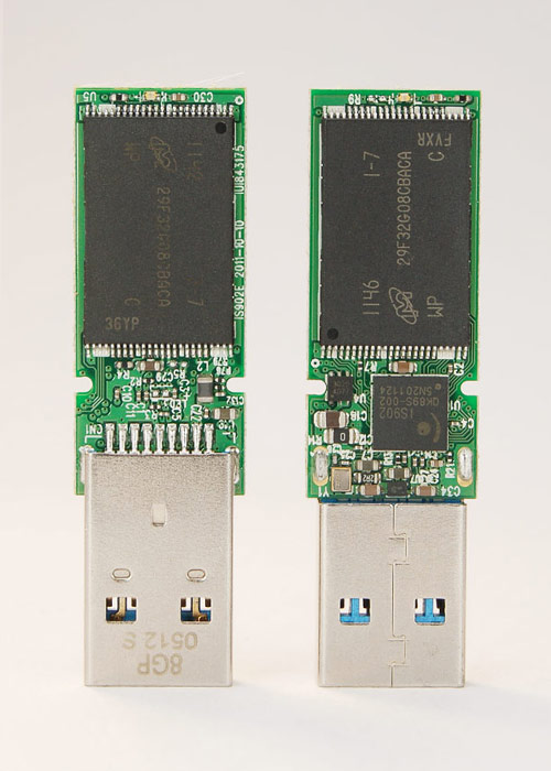
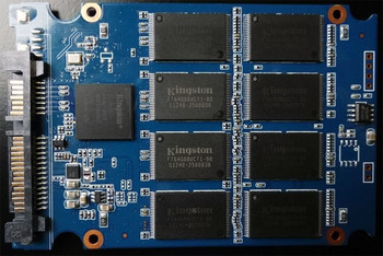
The internals of some typical USB thumb drives are shown in
figure 3 and figure 4. The word is
that the “vast majority of USB devices will accept any firmware
update they’re offered” according to
http://arstechnica.com/security/2014/07/this-thumbdrive-hacks-computers-badusb-exploit-makes-devices-turn-evil/
Here are some tools to inject code into certain off-the-shelf USB
sticks:
https://github.com/adamcaudill/Psychson/blob/master/README.md
Some discussion of the idea, including security ramifcations:
https://srlabs.de/badusb/
https://srlabs.de/blog/wp-content/uploads/2014/07/SRLabs-BadUSB-BlackHat-v1.pdf
At this point we need to mention some properties of present-day NAND flash technology. We restrict attention to SLC (single-level cell) technology, although similar words apply to MLC (multi-level cell) technology.
There are some special cases (including privacy-related cases) where rewriting a chunk is definitely worthwhile. There are ways of dealing with these cases, but details are beyond the scope of this document.
There is a tradeoff:
| Smaller ECC chunks allow for more flexible addressing. In particular, there is an incentive to match the LBA sector size. | Larger ECC chunks allow for more efficient error correction. |
Specific proposal: I suggest the following operational rule: Whenever a sensitive page becomes invalid for any reason, all the bits in the page should be programmed to the S state as soon as possible.
It is not required that the page be erase immediately, only that it be obliterated, i.e. programmed to the all-S state.
Note that in the long term, obliteration does not waste any resources. It merely reschedules work that needed to be done anyway. That is to say, it means preconditioning happens sooner rather than later.
Analysis:
In the long run it’s the same amount of work either way, but if the traffic is bursty, the non-privacy-enhanced system has the advantage that it can postpone the obliteration until the system is less busy.
In the simplest implementation, all pages on the device would be considered “sensitive” and would be treated the same. As a possible optimization, some subset of pages would be considered sensitive. Only the sensitive pages would be subject to the obliteration requirement.
Preferably, the concept of sensitivity should be a property of the logical data, not a property of the on-chip location.
If the privacy-enhanced storage is portable, so much the better. Examples include phones, USB sticks, SD cards, et cetera, with privacy-enhanced drivers and controllers built in.
On the other hand, the privacy-enhances storage does not really need to be portable, because the functions of portability and privacy enhancement can be separated. One possiblity would be to transfer some number of non-privacy-enhanced SD cards ... possibly one card, possibly thousands at once. The transfer can be protected by concealment. The transfer can also be protected by tamper-evident packaging.
Copy the pad data from the SD card to the privacy-enhanced memory device. Then destroy the SD card. One option is to grind it to dust. Other options include using heat and/or chemistry, which might make sense for bulk destruction, but not for onesy-twosy situations. In any case, the point is to make sure that before the pad is used for encoding or decoding, there are no extra copies lying around. There should be one copy for the sender and one copy for the receiver, period.
Eventually, every mass storage device will fail. It’s the nature of the beast.
Let’s consider flash memory in particular. Sometimes (albeit not always) the on-chip charge-pump will fail. This means it is no longer possible to erase the chip (to all ones) nor to program it (to all zeros). In other words, the chip becomes read-only, whether you like it or not. If you throw out such a chip and the adversary snatches it out of the trash, it’s a tremendous loss of privacy.
In other cases, it becomes no longer possible (or no longer reliable) to read the chip via normal methods. It is not safe to throw out such a chip, because the adversary may be able to read it using non-normal methods, including things like electron microscopes.
Here is a reasonably convenient way of destroying a chip, so that you can throw it out without worrying about it.
If you start with something bigger, such as a USB thumb drive or a an SSD drive, it will contain a circuit board with chips, as in figure 4. You need to remove the flash chip from the board. If it’s socketed, it should be easy to extract. If it’s soldered, you can unsolder it by heating it to about 200 ∘C and lifting it with a thin blade, such as a putty knife or perhaps a small flat screwdriver. It helps to hold the circuit card in a vice during this operation. A MAPP-gas torch will produce the required heat very quickly. Alternatively, a natural-gas flame (as on a cooking stove) is hot enough. A candle flame is hot enough.
Lately I’ve been seeing chips made of some sort of ceramic packaging material. It looks like epoxy, but it isn’t. Perhaps it is ceramic-filled epoxy. For such things, my procedure is to set the chip on a fire-resistant brick and use a MAPP-gas torch to heat it until it glows red-hot. It does not burn. After it cools it is very brittle, and turns to dust at the slightest touch, so the die comes out easily. Red heat will not melt silicon.
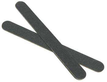
For highly sensitive operations, it might make sense to standardize on micro-SD cards, just because they make it super-easy to extract the die from the packaging. You can travel with an emery board in your luggage without arousing the slightest suspicion.
Consider an SSD, perhaps like the one shown in figure 9. Suppose it fails in such a way as to make one or more of the memory chips unwriteable. Even if only one chip has failed, it is probably not feasible to replace just that one. Full-disk encryption might be a big help here, as discussed in section 4.4, but if you don’t trust it – for example if you are worried about the security of the encryption key – the safest thing is to destroy all the chips.
If you happen to have an angle grinder, belt sander, disk sander, or similar power tool, you may be able to skip a step or two. That is, you might be able to grind away the chip packaging, possibly without removing the chips from the circuit board.
I have a hard time imagining a scenario where anything other than grinding would make sense.
However, if you insist on reducing the whole die to slag, you are better off using a combination of modest chemicals plus relatively modest temperatures ... rather than exotic chemicals separately or exotic temperatures separately. In particular, you can reduce an IC to slag using a temperature that is readily achievable with a MAPP-gas torch (cheap at any hardware store) in combination with baking soda (ridiculously cheap at any grocery store). It’s not particularly difficult, but still it’s an order of magnitude more work than simple grinding.
If you just make the die red hot for a minute or so, I would expect that to completely erase flash memory. The main drawback is that the die doesn’t look significantly different before and after, so it might be hard to verify to a third party that you did it correctly. In contrast, grinding is at least as easy to carry out, and incomparably easier to verify.
Even-less-practical possibilities include etching it with warm hydrofluoric acid or zapping it in a microwave oven. I’ve tried all these methods. They are somewhat amusing. However, they are vastly more work, especially if you include the setup beforehand and the cleanup afterwards.
Remember that you only need to grind away a few microns from the surface; you don’t need to annihilate the entire die.
If there is full-disk encryption, if you trust the implementation, it suffices to destroy the key. I’m not saying that I trust any disk vendors to implement it properly, but let’s temporarily and hypothetically suppose that they did, as follows:
Non-hypothetically speaking, I have zero confidence that disk vendors (SSD or otherwise) have implemented such a thing correctly. I can’t even get the Linux folks to implement a decent RNG that would allow “live CD” images to operate securely.
“Exploration and Exploitation of an SD Memory Card”
30th Chaos Communication Congress
video: https://www.youtube.com/watch?v=r3GDPwIuRKI [1 hour]
slides: http://bunniefoo.com/bunnie/sdcard-30c3-pub.pdf
Copyright © 2015 jsd