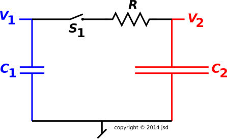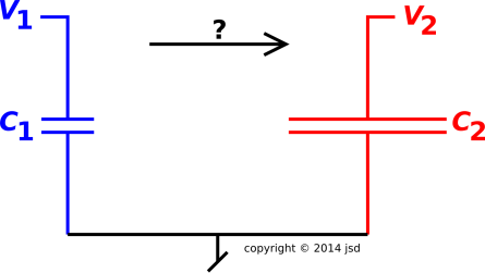
Figure 1: Two Capacitors
It is quite possible to transfer energy and charge (or rather gorge) from one capacitor to another with high efficiency. The energy-transfer efficiency can approach 100%, and the gorge-transfer efficiency can easily exceed 100%. These numbers far surpass the limits that are often assumed, “proved”, and/or “explained” in the physics education literature. We discuss a simplified version of a technique that is very widely used in the electronics industry.
Let’s consider the so-called “Two Capacitor Problem”.
Suppose we have two capacitors, as shown in figure 1. Initially there is some energy stored in the left capacitor (shown in blue) but zero energy in the right capacitor (shown in red). The objective is to transfer “some” energy from one to the other.
Without loss of generality, assume the right capacitor has N times the capacitance of the left capacitor:
| (1) |
Figure 2 shows one scheme for performing the transfer. When the switch is closed, a current flows.
Under this scheme, elementary circuit analysis tells us that the final voltage is:
| (2) |
The energy is proportional to the capacitance and the square of the voltage, so the final energies are:
| (3) |
The subscript “12” refers to the whole system, i.e. both capacitors together.
We can also take a look at the gorge on the capacitors. (All-too-often people call this the “charge” on the capacitors, but that is a misnomer, as discussed in reference 1.)
| (4) |
This works, but as we shall see, it is not the only possible scheme. Indeed it is nowhere close to being the optimal scheme.
The most remarkable thing about equation 3 is that the results are independent of R. So in some sense this a “universal” result.
One might even imagine that equation 3 remains valid even when R=0. However, this doesn’t make sense, because the dissipated energy is dissipated in the resistor. This is the infamous two-capacitor “paradox”.
The usual way of resolving this “paradox” is to argue that there is always some parasitic resistance (not shown in the circuit diagrams), so that in the limit where the explicit resistance R goes to zero, the parasitic resistance becomes dominant. If nothing else, there will always be some radiation resistance.
A tremendous amount of effort has gone into “proving” that this result is universal, and/or “explaining” why it is mandatory, and/or accounting in detail for the “lost” or “missing” energy. I would argue that all of this work is seriously misguided, because in fact the result is not universal and not mandatory.
In passing from figure 1 to figure 2, we added a switch and an explicit resistor. You could also add a parasitic resistor and/or an antenna to represent radiation resistance. However, there is no law of physics that says these are the only possibilities. The same physics that allows us to understand capacitors, resistors, switches, and radiation also allows us to understand inductors.
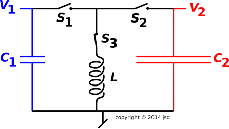
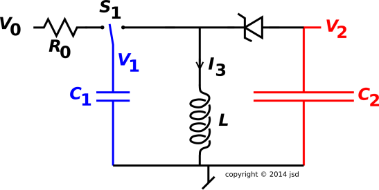
A particularly interesting possibility is to add an inductor and some switches, as shown in figure 3. Switch S3 is normally closed, and will remain closed until further notice.
Proper operation of this circut requires some deft timing, as we now discuss.
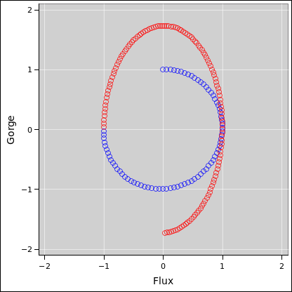
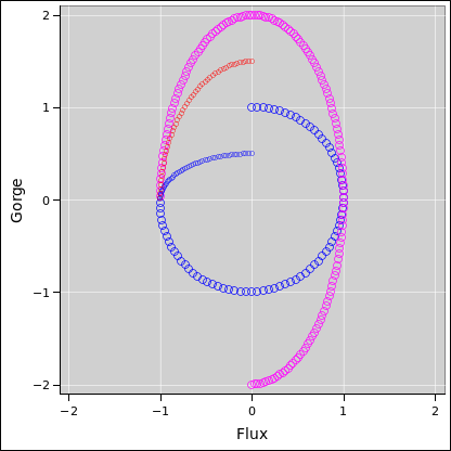
We start by closing the left switch (S1), connecting C1 to the inductor. This creates an LC oscillator, a simple harmonic oscillator. The initial condition is shown by the highest point on the blue trace in figure 4. We call this the 12:00 point on the blue trace.
The spreadsheet used to compute the waveforms and phase-space plots in this document is cited in reference 2.
After waiting a quarter of a cycle, the system has evolved to the 3:00 point. All of the energy has been transferred from C1 to the inductor. This is interesting, but not maximally convenient, because the current in the inductor is flowing in the “wrong direction” for our purposes. However, if we wait an additional half cycle, the system will evolve to the 9:00 point, where the current is flowing in the desired direction.
At this point we open the left switch (S1) and close the right switch (S2) connecting the inductor to C2. This creates a different LC oscillator, with a different period. The new period is longer than before by a factor of √N.
At this point in the diagram, the trace switches from blue to red. Now we wait an additional quarter period, i.e. a quarter of the new period. This takes us to the 12:00 point on the red trace. At this point – assuming ideal components – all of the energy has been transferred to C2.
| (5) |
| (6) |
We should also look at the gorge:
| (7) |
In particular, comparing with equation 4, we find that this scheme produces more gorge on C2 by a factor of (N+1)/√N ... which is a factor of 2 already when N=1 and gets even bigger for large N.
Let’s be clear: In the circuit we are considering here, i.e. figure 3, we wind up with more gorge than we started with, for any N greater than 1 ... not only more final gorge than we would have gotten with figure 2, but more than we started with. There is no law of physics that requires gorge to be conserved.
You may have noticed that in figure 2 the final gorge was equal to the initial gorge, but this is not a consequence of any deep physical law; it is merely the consequence of some engineering choices that were made ... not even particularly clever engineering choices.
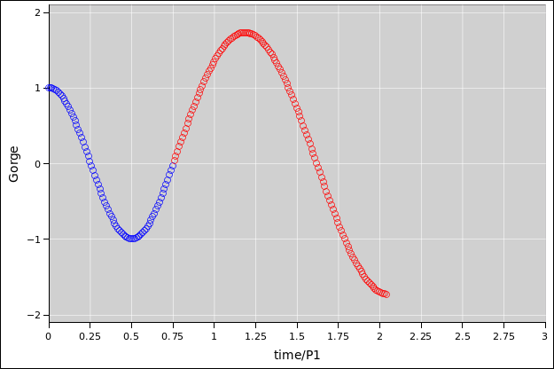
In addition to the phase-space plot in figure 4, we can get some additional insight by looking at the waveforms as a function of time, as in figure 5.
The ordinate is the gorge on both capacitors combined. However, the capacitors take turns, so the blue part of the trace represents the gorge on C1, while the red part represents the gorge on C2.
The abscissa is time, measured in units of the period of the “blue” LC oscillator, namely
| (8) |
The period of the “red” LC oscillator (P2) is longer by a factor of √N, but this has no bearing on the units used for the abscissa in the plot. Note that to make the diagrams, the value N=3 was chosen.
Note that a full cycle of the red trace in figure 5 is identical to a full cycle of the blue trace, just scaled up by a factor of √N ... scaled up in both the gorge-direction and the time-direction. As a corollary, the slope is the same at corresponding points. In particular, at the point where the red trace splices onto the blue trace, there is no change in slope.
We can understand this in physics terms as follows: The time-derivative of the gorge is the current. At the splice-point, we are switching the current from one capacitor to the other, but it is the same current, so the slopes have to match.
As a further point of physics, we have chosen to do the splice at a point where there is zero voltage across the inductor, so in accordance with the following equations
| (9) |
not only do the gorge-traces match as to slope, they also match as to second derivative. They both have zero second derivative, i.e. zero curvature. The chosen splice-point is an inflection point.
Here is a third way of understanding the scaling relationship. It follows from the Maxwell equation. There is some current flowing in the inductor. If the voltage is less, the current flows for a longer time.
Let’s change gears slightly. Suppose that rather than transferring all the energy from C1 to C2, we only want to transfer enough so that the two capacitors come into equilibrium, i.e. so that they have the same voltage. We can do this using the same circuitry as in figure 3, just using different timing.
Everything is the same as in section 3 for the first three quarters of a cycle, up to the point where we throw the switches.
Recall that at the 9:00 point on the blue trace, both capacitors are at zero voltage. In this case, we leave switch S1 closed when we close switch S2. Thereafter the two capacitors remain locked together, with a common voltage.
The period of the combined oscillator (P12) is longer than the reference period by a factor of √1+N. To make the diagrams, the value N=3 was chosen, so P12 = 2 P1.
In figure 6, the magenta trace represents the combined system, blue and red together. When the magenta trace reaches 12:00, all the energy is in the capacitors, not the inductor. At this point we can open switch S3 and the capacitors will remain in equilibrium with each other. (The magenta trace in the diagram continues past this point, but if all you wanted was to establish equilibrium you would not allow the oscillations to continue.)
In figure 6 and also in figure 7, the behavior of C1 and C2 separately are shown beyond the splice point, using small blue and red circles. They are rather less interesting than the total system behavior.
The key results are:
| (10) |
| (11) |
| (12) |
We can also look at the waveforms as a function of time.
Again there is a scaling law: The magenta curve is a scaled-up version of the blue curve, scaled in both the time-direction and the gorge-direction.
This stands in contrast to power supplies using dissipative elements in series. Such devices are similar to figure 2, but with a transistor in place of the resistor. Such devices exist, and used to be very common, but they are very inefficient, and became obsolete several decades ago. Back in the bad old days, the power supply for a computer would be a significant fraction of the size and weight of the whole computer, and would be responsible for a goodly fraction of the energy budget (and also the cooling budget).
Many DC-to-DC converters are also known as buck/boost regulators, alluding to the fact that the same circuit can handle input voltages that are greater than or less than the desired output voltage, which is something that would be hard to achieve using a plain old dissipative Class-A regulator.
Such circuits are available in a wide range of sizes, from a few milliwatts to a few gigawatts. Applications at the small end include LED flashlights. Applications at the large end include HVDC power lines that carry power to entire cities. Note that DC is sometimes significantly more efficient than AC for long-distance power distribution, especially if the cables run underwater.
Many sports use something like a bat or a racquet to make energy transfer more efficient. Mechanical weapons such as a slingshot or a bow-and-arrow depend on efficient transfer of energy.
The idea of an impedance-matching transformer is in some ways different but in some ways related.
Note the contrast:
| The operation of the circuit in figure 2 is simple. You can throw the switch and then go get lunch. The capacitors will come into equilibrium and then stay in equilibrium while you are gone. | The operation of the circuit in figure 3 is much more complex. You have to open and close various switches at various times, and the timing is critical. |
| The circuit in figure 2 can easily be demonstrated in an introductory physics class. | The circuit in figure 3 is much more energy-efficient, but it is not convenient to demonstrate. It requires a great deal of supporting circuitry to get everything to work right. |
We can split the difference using the circuit shown in figure 8. Compared to figure 3, this circuit is much easier to operate. It is not quite as energy-efficient, but still much more efficient than figure 2. In particular, for large N, more than 100% of the gorge on capacitor C1 gets transferred to capacitor C2.
In this circuit, S1 is a double-throw center-off switch. The first step is to switch S1 to the left, so that capacitor C1 gets gorged up and V1 becomes equal to the applied voltage V0. We assume V0 is positive. We are not interested in the details of where V0 comes from; that is considered external to our circuit. Similarly R0 is considered external and not part of our efficiency calculation; it is just there for safety, to make sure the inrush current is not infinite when S1 is switched to the left. Our analysis begins after C1 has been gorged up; we want to see how efficiently energy and gorge can be transferred from C1 to C2.
The second step is to switch S1 to the right. This forms an LC circuit involving C1 and L. At this moment, C2 is not involved, since the diode is reverse biased and therefore non-conducting.
However, a short time later, the natural LC oscillation will bring the voltage V1 into negative territory. The diode is now conducting. If we arrange that the forward drop of the diode is negligible compared to the other voltages, the circuit is now equivalent to figure 3 with all three switches closed.
The voltage V2 will be negative, opposite to the sign of V1. This is slightly inelegant, but it is part of the price we pay for having a circuit with a low parts count and simple operating procedure.
After capacitor C2 is fully gorged, the diode will stop conducting. The LC circuit formed by C1 and the inductor will continue to oscillate with a small amplitude, less than one diode-drop.
At some point you will want to open switch S1. Ideally this should be done at a point in the cycle where the current I3 is positive, where the positive direction is “downward” as defined by the circuit diagram. However, this sort of fine timing is contrary to the spirit of ultra-simple operation. Therefore the recommended procedure is to simply wait until the LC1 oscillations have died out (due to the inevitable parasitic dissipation) before flipping the switch.
Another possibility is to use a Zener diode, where the Zener breakdown voltage is larger than V0. This protects the diode against the possibility that somebody might throw the switch in such a way that the inductor tries to force current through the diode the wrong way.
Consider the scenario where V0 = 24V and N = C2/C1 = 10. In this scenario, the circuit in figure 8 (compared to figure 3) delivers 3× more gorge and 3× more energy to the output capacitor C2. For larger values of V0 the advantage is even greater, because the diode-drop is less of an issue. Also larger values of N make the advantage even greater.
In any case, the fundamental physics point remains: It is possible to transfer energy and gorge from one capacitor to another with very high efficiency.
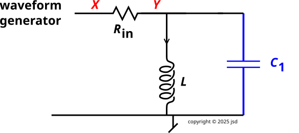
If you don’t have an RLC meter available, you can hook up the circuit shown in figure 9; that is, a parallel LC circuit driven from a high impedance, namely Vin. (High means large compared to the parasitic series resistance of the inductor, which you can measure with a low-tech ohmmeter). Measure the resonant frequency and Q of the LC combination. If the Q is not reasonably high, the circuit won’t work well, and you need to get a better inductor.
Check both LC1 and LC2 just to be sure.
If it’s not obvious how to find the resonance, use your oscilloscope in XY mode to draw a Lissajous pattern.
Note that a lot of smart people have gotten this wrong over the years. A lot of people assumed – or even “proved” that the results in equation 3 were mandatory and universal. Let this be a warning: Just because you cannot think of a better way of doing things does not prove that no better way exists!
The advanced student may find it instructive to go over the various “proofs” and make a list of the false assumptions that went into them. It is a long list. Here are a few examples
And so on......